Semiconductor
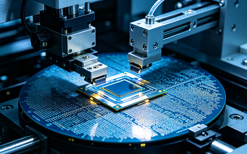
1、 Scenario positioning: Covering the foundry needs of the entire semiconductor industry chain
Deeply cultivating the four core areas of wafer manufacturing equipment, semiconductor packaging and testing, high-end semiconductor devices, and third-generation semiconductors (SiC/GaN), we provide full process outsourcing services from core component processing to whole machine OEM for key products such as lithography equipment core components, wafer carriers, power device packaging structures, and semiconductor testing instruments, helping customers overcome industry pain points such as high hardness material processing, nanometer level precision control, and clean production, and accelerating the localization of semiconductor equipment.
2、 Core solution: Six major services targeting pain points in the semiconductor industry
1. Precision machining: semiconductor core component solution with atomic level precision
Scenario adaptation: Lithography equipment workbench, wafer cutting tool holder, SiC/GaN substrate fixture, semiconductor detection probe holder
Technical highlights:
Tolerance control up to ± 0.0001mm (nanometer level standard), compatible with Mohs 9 high hardness materials such as SiC and GaN, breaking through the pain points of traditional process edge breakage and microcracks
Equipped with a five axis linkage machining center and an online electron beam measurement system, it achieves complex surface machining with a cutting error of ≤ 0.1nm, meeting advanced process requirements of 5nm and below
By adopting low damage cutting technology, the heat affected zone (HAZ) is controlled within 5 μ m, and the utilization rate of SiC wafer material is increased to over 90%, with the edge breakage rate reduced to below 1%
Full batch material traceability (including MTR material certification), in compliance with the full process process process record requirements of SEMI S2-0724E standard
2. Sheet metal processing: customized solution for structural components of clean grade semiconductor equipment
Scenario adaptation: semiconductor equipment rack, wafer transfer chamber, clean room partition, testing instrument casing
Technical highlights:
Select 304L stainless steel and aviation grade aluminum alloy, and use precision laser cutting (accuracy ± 0.03mm) and bending (accuracy ± 0.1mm) processes to ensure that the assembly gap of structural components is ≤ 0.05mm
Production in ISO Class 5 cleanroom (dynamic particle count ≤ 3520 particles/m ³), all components are wiped with 75% isopropanol and purified by air shower to avoid particle contamination
Anti static structure design, surface grounding resistance ≤ 1 Ω, in compliance with semiconductor AMC molecular pollutant control standards, suitable for wafer process electrostatic protection requirements
Modular splicing process, no silicon sealing treatment at the joints, meeting the sealing requirements of clean room pressure difference ≥ 10Pa
3. Surface treatment: Clean grade functional coating solution
Scenario adaptation: wafer carriers, semiconductor equipment contact surfaces, power device heat dissipation substrates, electrostatic protection components
Technical highlights:
Clean level coating process: silicon free anti-static coating (surface resistance 10 ⁶ -10 ⁹ Ω), DLC diamond-like coating (hardness ≥ 2500HV), to avoid particle detachment and wafer contamination
Corrosion resistant and wear-resistant treatment: using chromium free passivation+vacuum coating process, salt spray test for more than 1000 hours, suitable for semiconductor corrosive chemical environment
Thermal management optimization: For the heat dissipation substrate of SiC power devices, laser cladding high thermal conductivity coating is adopted, and the thermal conductivity is increased to above 200W/(m · K)
Coating thickness tolerance control ± 2 μ m, meeting the dimensional consistency requirements of semiconductor precision assembly, and free of volatile organic compounds (TVOC ≤ 500 μ g/m ³)
4. Electrical R&D support: SEMI compliant semiconductor electrical system solution
Scenario adaptation: semiconductor equipment control system, detection instrument PCBA, wafer transfer servo drive module
Technical highlights:
Complies with SEMI S22 electrical safety standards, adopts double insulation design, grounding resistance ≤ 0.1 Ω, leakage current 5mA, emergency stop system adopts electromechanical hard wire control
Deep optimization of electromagnetic compatibility (EMC), radiation interference limit ≤ 30dB μ V/m, meeting SEMI F47 voltage sag anti-interference requirements, avoiding interference with chip processes
High stability design: Embedded software supports real-time calibration of process parameters, servo system positioning accuracy reaches ± 0.001mm, suitable for high-precision control scenarios such as wafer transfer and photolithography alignment
High temperature environment adaptation: Electrical components have a temperature resistance range of -40 ℃~125 ℃, meeting the operational stability requirements of semiconductor equipment in high-temperature processes
5. Complete assembly OEM: Clean grade whole machine OEM full process control plan
Scenario adaptation: semiconductor testing instruments, small wafer processing equipment, third-generation semiconductor device packaging equipment
Technical highlights:
ISO Level 5 cleanroom assembly, implementing full process control of "component purification assembly leak detection cleanliness testing", with particle contamination of the entire machine ≤ 10 particles/㎡ (≥ 0.5 μ m)
Support flexible production, quickly switch between small-scale trial production (minimum order quantity of 5 units) and large-scale mass production (daily production capacity of 200 units), and adapt to the iterative needs of semiconductor equipment
Includes IQ/OQ/PQ process validation, provides complete equipment history records (DHR) that comply with SEMI standards, and helps customers quickly pass international certifications
Modular assembly design, equipped with specialized anti-static tools and grounding testing points, with one grounding detection terminal set every 50 square meters to ensure that the static protection of the entire machine meets the standard
6. Customization of Finished Products: Implementation Plan for Third Generation Semiconductor Innovative Devices
Scenario adaptation: SiC power device packaging structure, GaN RF device, ultra-thin wafer processing fixture, customized semiconductor testing fixture
Technical highlights:
Collaborate with clients to optimize the processing technology for high hardness materials, achieving a defect density of ≤ 10 defects/cm ² for SiC substrates, meeting the requirements of automotive grade power devices
Provide full cycle services from prototype sampling (5-7 day fast delivery), process validation to mass production delivery, shortening the launch cycle of third-generation semiconductor products by more than 40%
Customization for extreme working conditions: specialized component processing for high temperature (above 2000 ℃) and high cleanliness scenarios, such as SiC crystal growth furnace core components
Support cross process integration, such as integrated customization of precision mechanical structures with semiconductor sensors and AI detection modules
3、 Compliance and Quality Assurance: Building a Secure Defense Line for the Semiconductor Industry
Qualification certification: ISO 9001 quality management system, ISO 14644-1 cleanroom certification, fully compliant with international semiconductor standards such as SEMI S2, S22, F47, etc
Clean production control: equipped with ISO Level 5 core processing workshop and ISO Level 7 assembly workshop, fully implementing anti-static, anti particle, and anti molecular pollution (AMC) control throughout the process
Detection capability: Equipped with professional equipment such as electron beam measuring instruments, particle counters, EMC testing systems, etc., the key indicator detection coverage rate is 100%, and the defect detection accuracy reaches 10nm level
Intellectual property protection: Establish a semiconductor technology confidentiality system, sign special confidentiality agreements, and encrypt and store customer design data and process documents throughout the entire process
4、 Collaboration Value: Becoming a Reliable Manufacturing Partner for Semiconductor Innovation
Technological breakthrough: Overcoming industry bottlenecks such as high hardness material processing, nanometer level precision control, and clean production, helping customers break through the barriers of advanced processes and third-generation semiconductor technology
Compliance reduction: Full process SEMI standard compliance assurance, providing complete process records and certification support, reducing customer international market access risks
Efficiency improvement: A rapid response mechanism from R&D trial production to mass production delivery, flexible production adapted to the fast iteration and large batch fluctuations of the semiconductor industry, and the capacity utilization rate increased to over 95%